Making a Brain PCB
10/27/2021
redraw an echo hello-world board,
add (at least) a button and LED (with current-limiting resistor)
check the design rules, make it, and test that it can communicate
So, I decided to go with the 10 pin D11C echo hello board. This was due to a combination of it being similar to the board I had made for the programming in Week 2 and that it seemed relatively simple to program given that I could find plenty of documentation and examples.
How would I actually redraw and make the PCB though? We had pretty much two options: Eagle and Kicad. Since I like open source and wanted to stay away from Autodesk, I went with Kicad. I'm also not doing very advanced design, so it didn't really matter. Kicad was pretty straightforward to download and install. The only additional step you need is getting the fab lab libraries: here. To mill it, we would be using the same SRM-20 we used on the earlier programmer board.
Designing the PCB
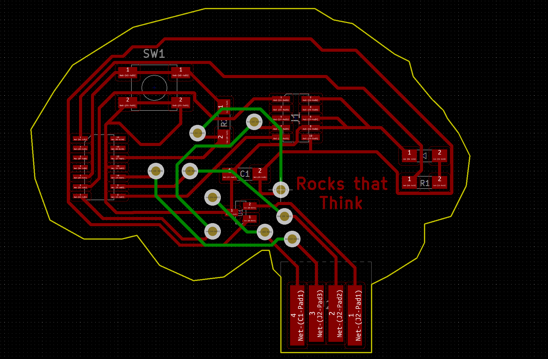
But because I'm in the same class as try-hard graduate students, I have to do something special. Relative to other weeks, I came up with my idea for this week pretty quickly. Follow with me here: computers... are like brains... so what if I made it in the shape of a brain?!11!! 🤯 For the extra step, I tried to lay out each component where the corresponding/analogous region in the brain is.
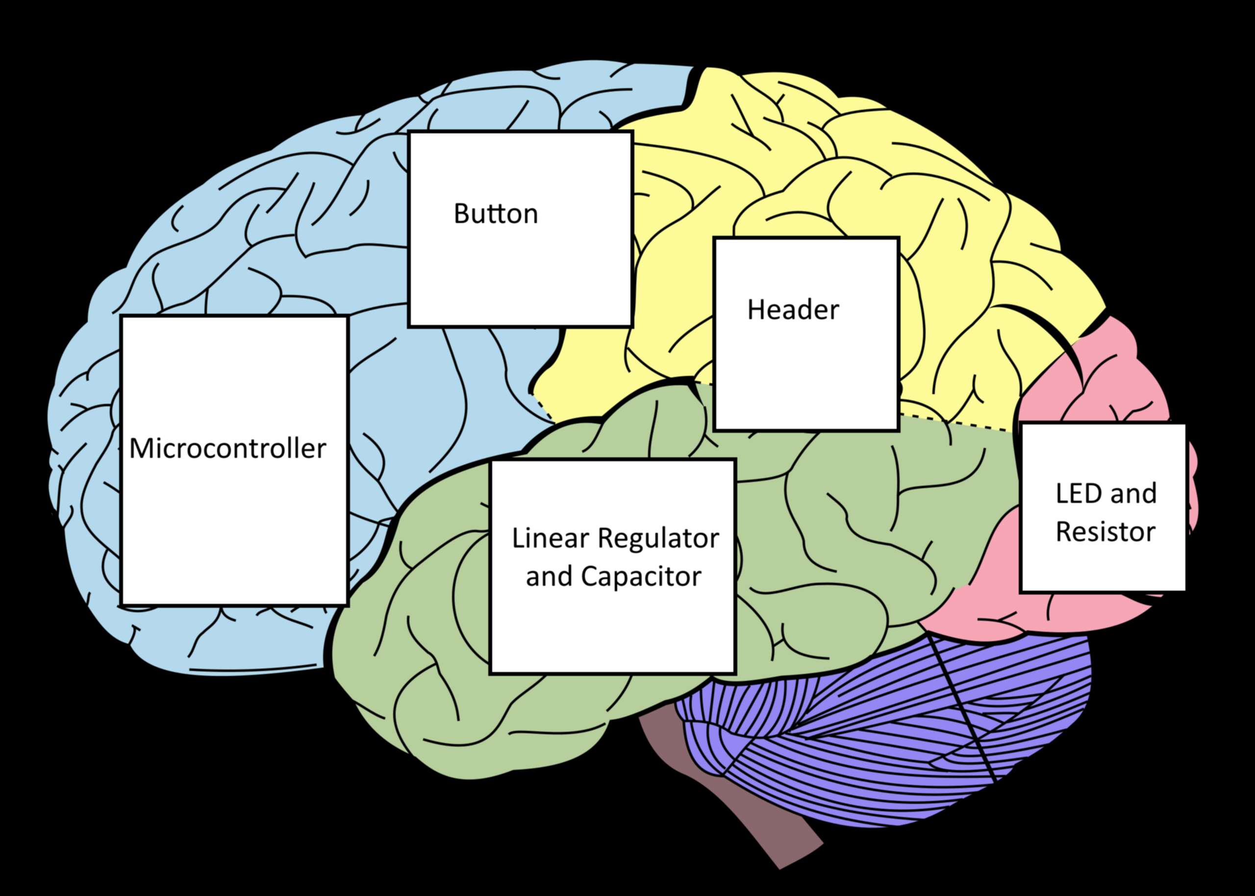
- SAMD11C Microcontroller - Frontal Lobe (higher level functions like thinking)
- Linear Regulator and Capacitor - Hypothalamus (homeostasis regulation)
- Resistor and LED - Occipetal Lobe (light perception)
- Button - also Frontal Lobe (decision making)
- Header - Wernicke's Area (language processing)
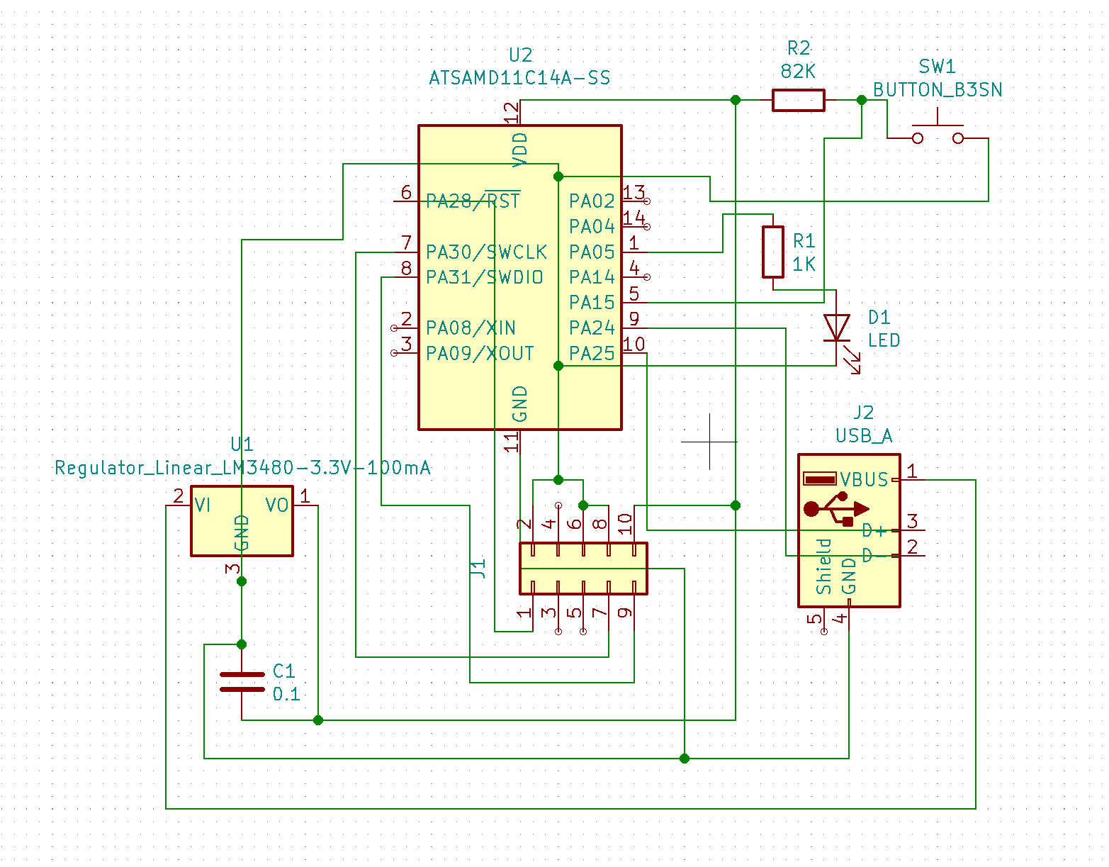
The first step in making a PCB is making a schematic. This is a representation of the connections that will exist in the final board. The wires drawn here have no physical nature to them, they are just to show what goes to what. All my job was to do is to add a button, resistor, and LED to an existing board design. So, I copied the D11C board echo hello board that I was redrawing, and then added a Button, LED, and resistor following: this super handy document. This got me the following messy schematic, which works because the wires aren't real.
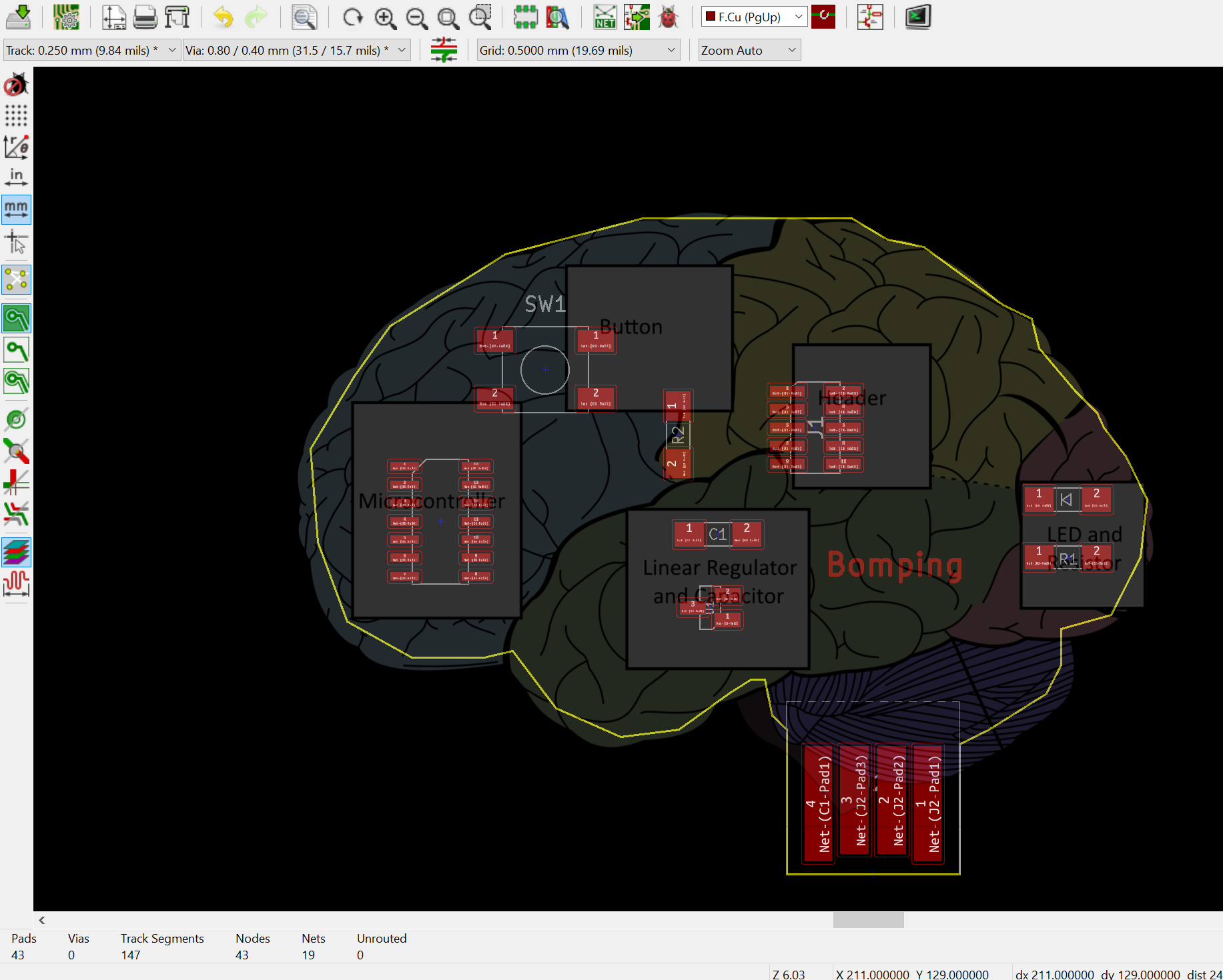
The next step in making a PCB is laying out the components with their real life footprint(physical representations). Foreshadowing, but could you see any downsides to putting the components in arbitrary places in a brain shape as opposed to where routing the traces makes the most sense? In hindsight, I should have also spent more time on rotating the footprints here but I'm not sure if it really mattered. I had to move the button further to the left to make it more forntal lobey. To overlay the schematic of the brain while I was doing this, I used a wonderful piece of free software called PureRef. It's great literally whenever you want to reference something while doing something else. In the end, here's what the laying out of the footprints looked like:
Now for the hardest part, routing the traces. The first step of the process is to setup the design rules, how thick the traces should be, how much clearance, size of holes, etc. Although I didn't know it at the time, when I exited, I guess I hit "Cancel" instead of "Ok", so my changes didn't save:

Continuing onwards, I went onto routing the traces. After about an hour of trying to figure out a way to do it without a 0 omh resistor, I figured out this design:
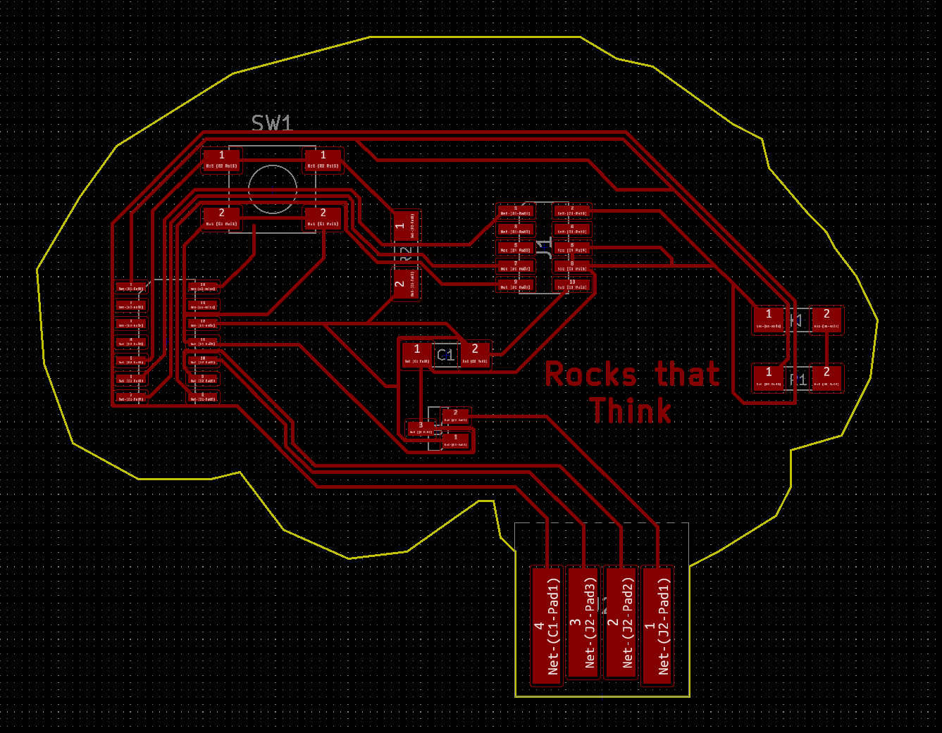
Any experienced people reading this can already tell this is off. The traces are absolutely tiny. However, I didn't notice this at this point because I still thought that I had entered in the design rules correctly. When I was loading the file into MODS, the cutting profile wasn't doing the little traces, so I knew something was wrong. So, I tried seeing what it would do if I ran MODS again using a 1/100th bit instead of a 1/64th, and the result cutting path showed more detail. At this point I knew that my lines were too small so I went back to my laptop to check what the issue was, and lo and behold, I found it: the design rules. So at midnight, when I thought I was almost done, I had to restart the problem and make it 4x harder. After properly setting the design rules, I could no longer fit three wires underneath a 1206 resistor, I could only do one. Still confident in my ability to make a design without a (or 20) 0 ohm resistor, I kept trying to figure out paths. Remembering that someone mentioned autorouting in the lecture and how it sucks, I thought I'd give it a go since I couldn't figure it out. So I downloaded FreeRouter and got this result:
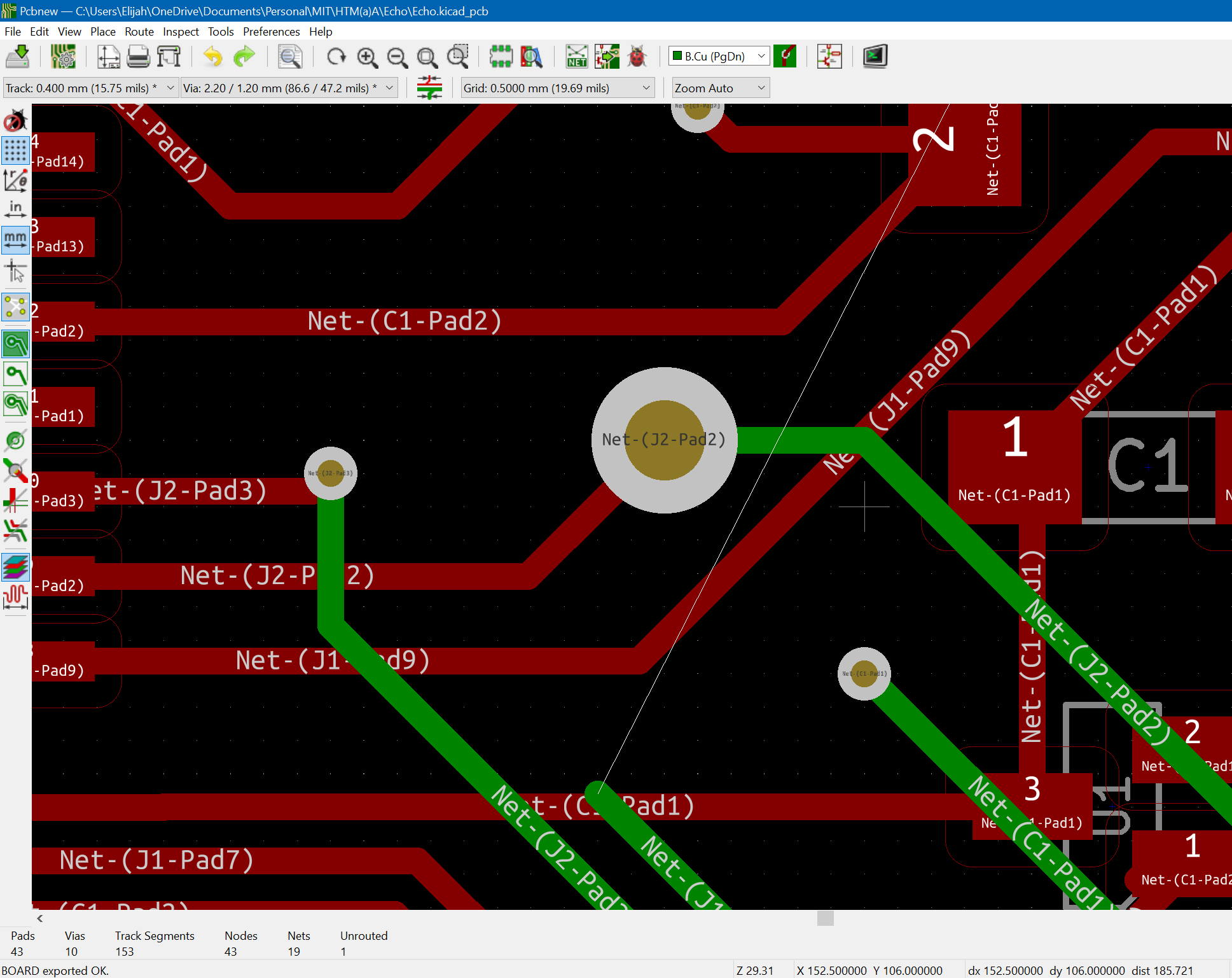
This was the final nail in the coffin of my simple design dream. If the computer couldn't figure out a way to solve the routing, than I wouldn't be able to. It did, however, show a pretty easy solution if I did a double-sided PCB though. Screw it, I'm already this far in, let's do double-sided! So I watched a short youtube video on how to add back traces in Kicad, and then essentially copied the autoRouter doing a bit of cleaning and decoration. After adding all the vias, I finally had a board that would work! However, I still hadn't realized that the final setting the the board setup menu was off, so my vias were all the wrong size. The small size is the size they were, and after a failed mill, the big size is the size they are supposed to be:
After making that last fix, at last I had the following file:
Making the PCB
Now that I had the source file, all I had to do was stick it into Inkscape and split it into the component procedures. Because I needed to mill both sizes of the board, the milling was a bit more complicated than it otherwise would have been.
- Front Traces 1/64 bit
- Holes 1/32 bit
- Box Outline 1/32 bit
- ###Flip
- Back Traces 1/64 bit
- Brain Shape 1/32 bit
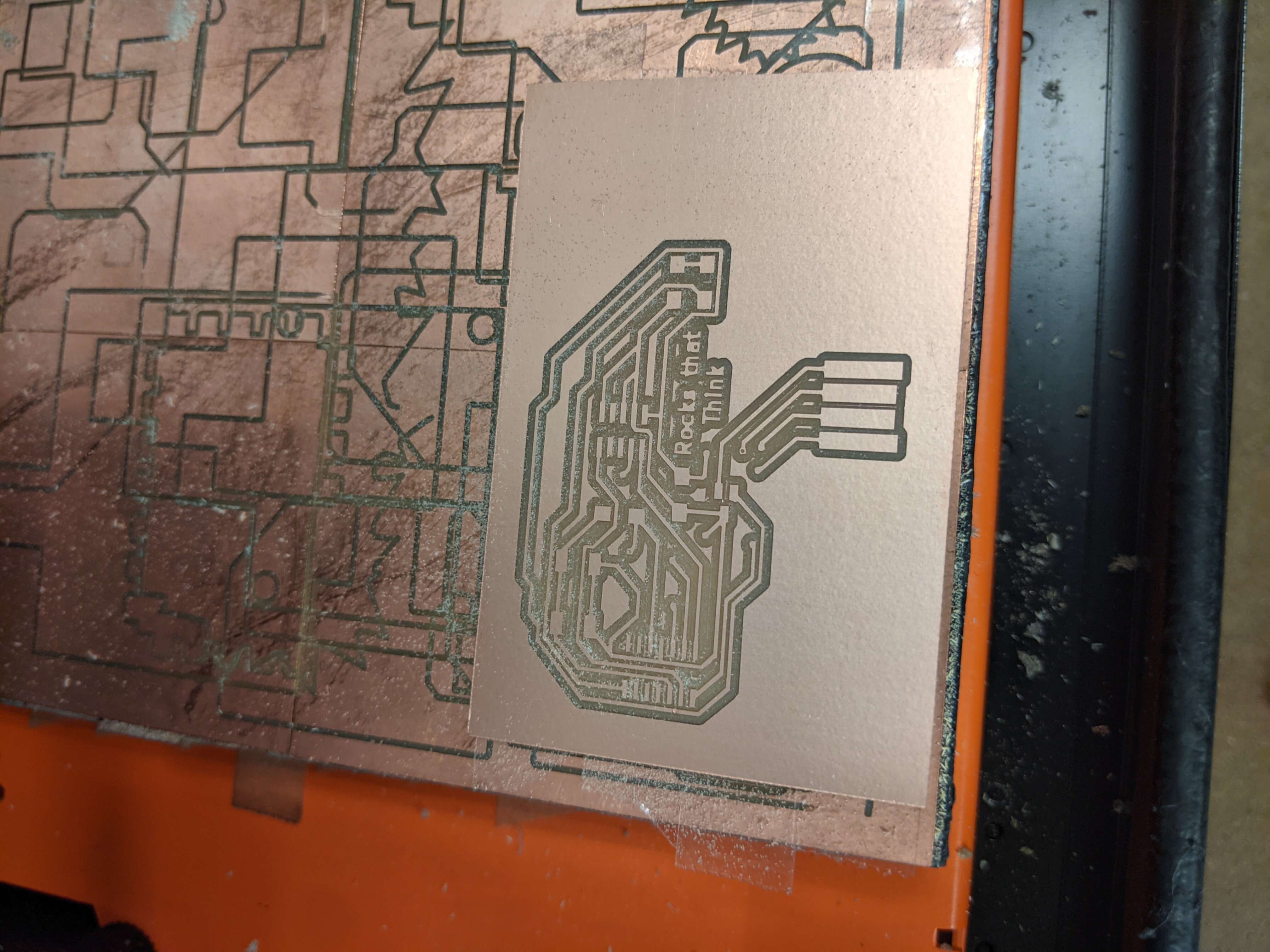
Now at last for the milling. In order to flip it over and get it to be referenced properly for the back traces and holes, I had to add a box around everything to make the flipping symmetrical. It makes sense if you look at these images and imagine turning the board over.
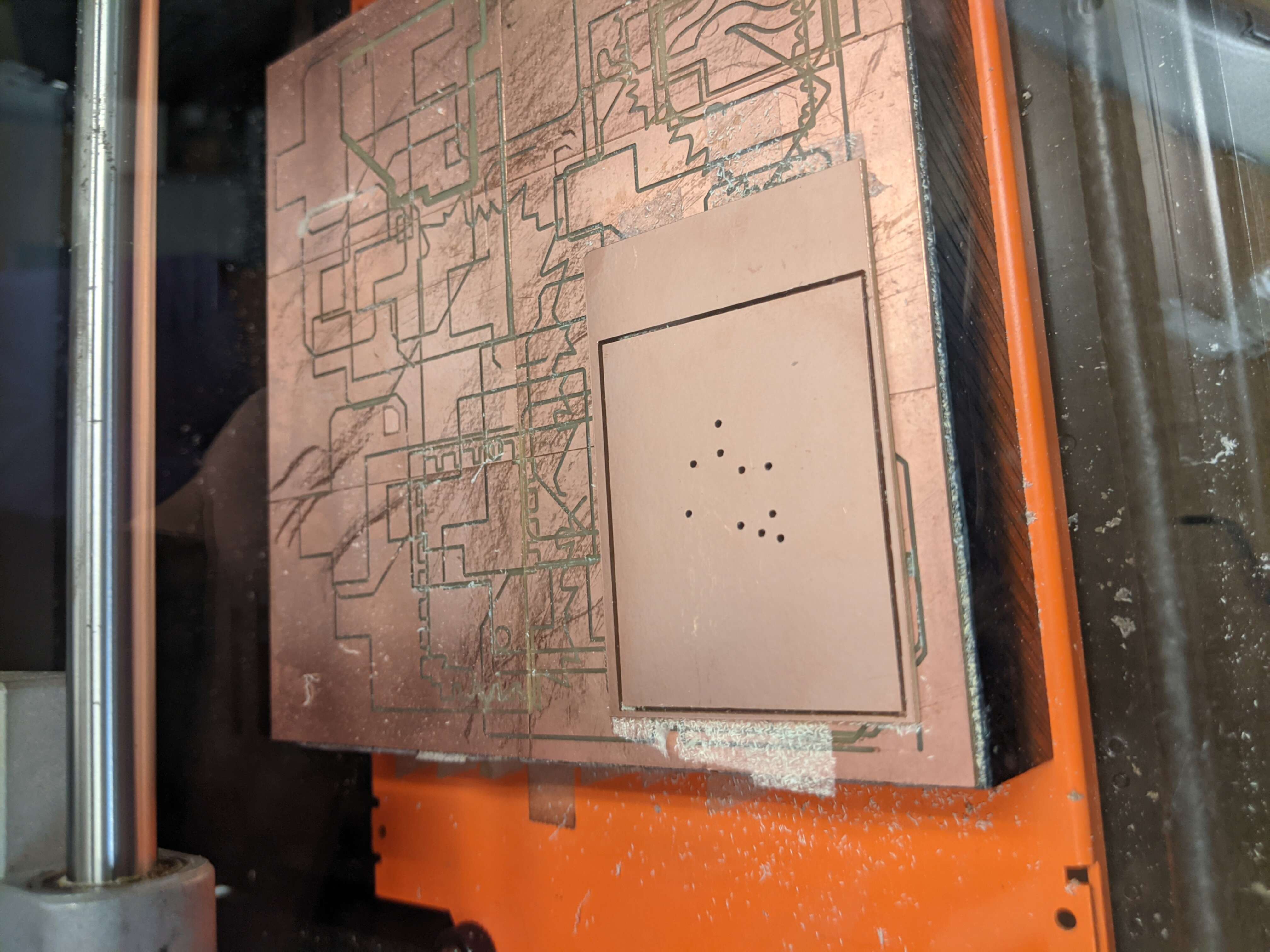
After flipping the board over and about to do the back traces:
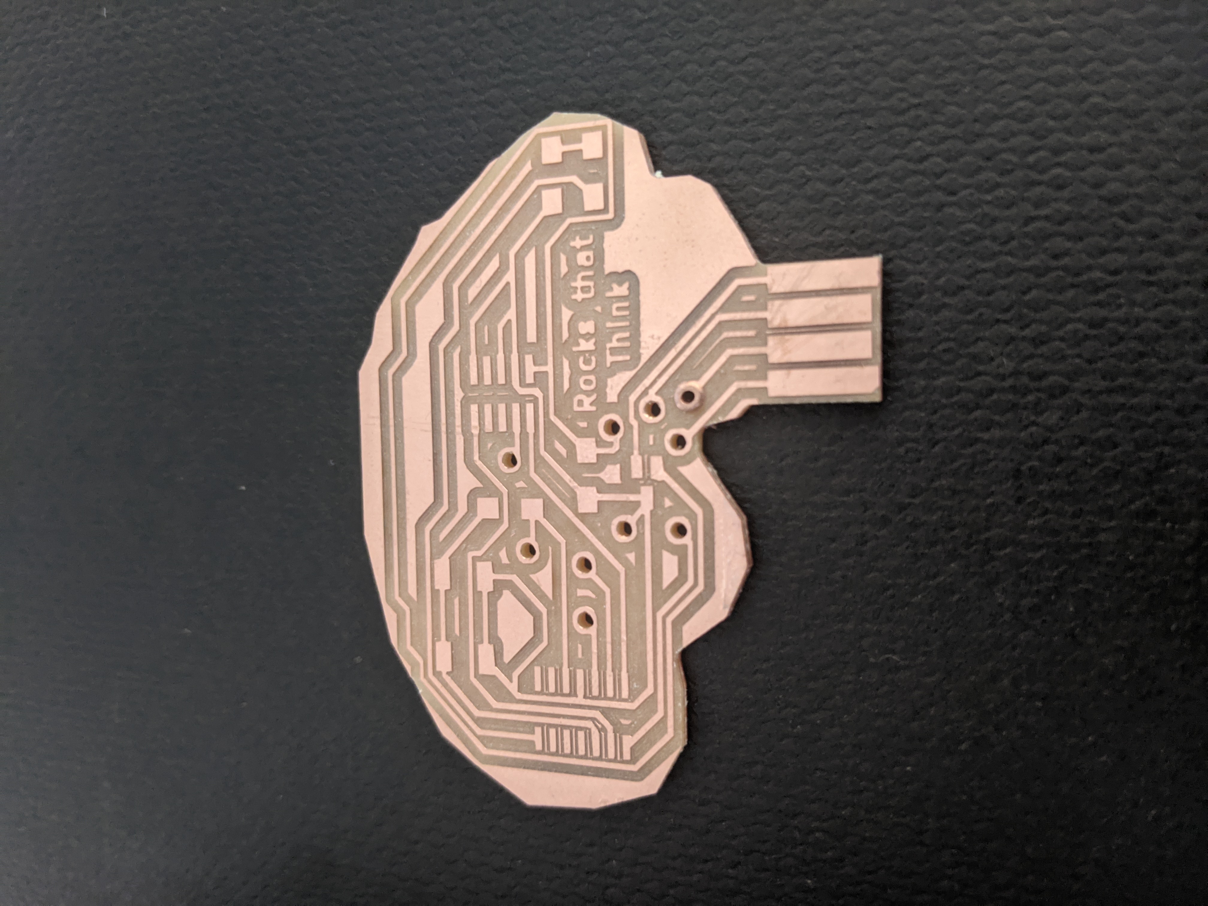
And, at last, the completed PCB:
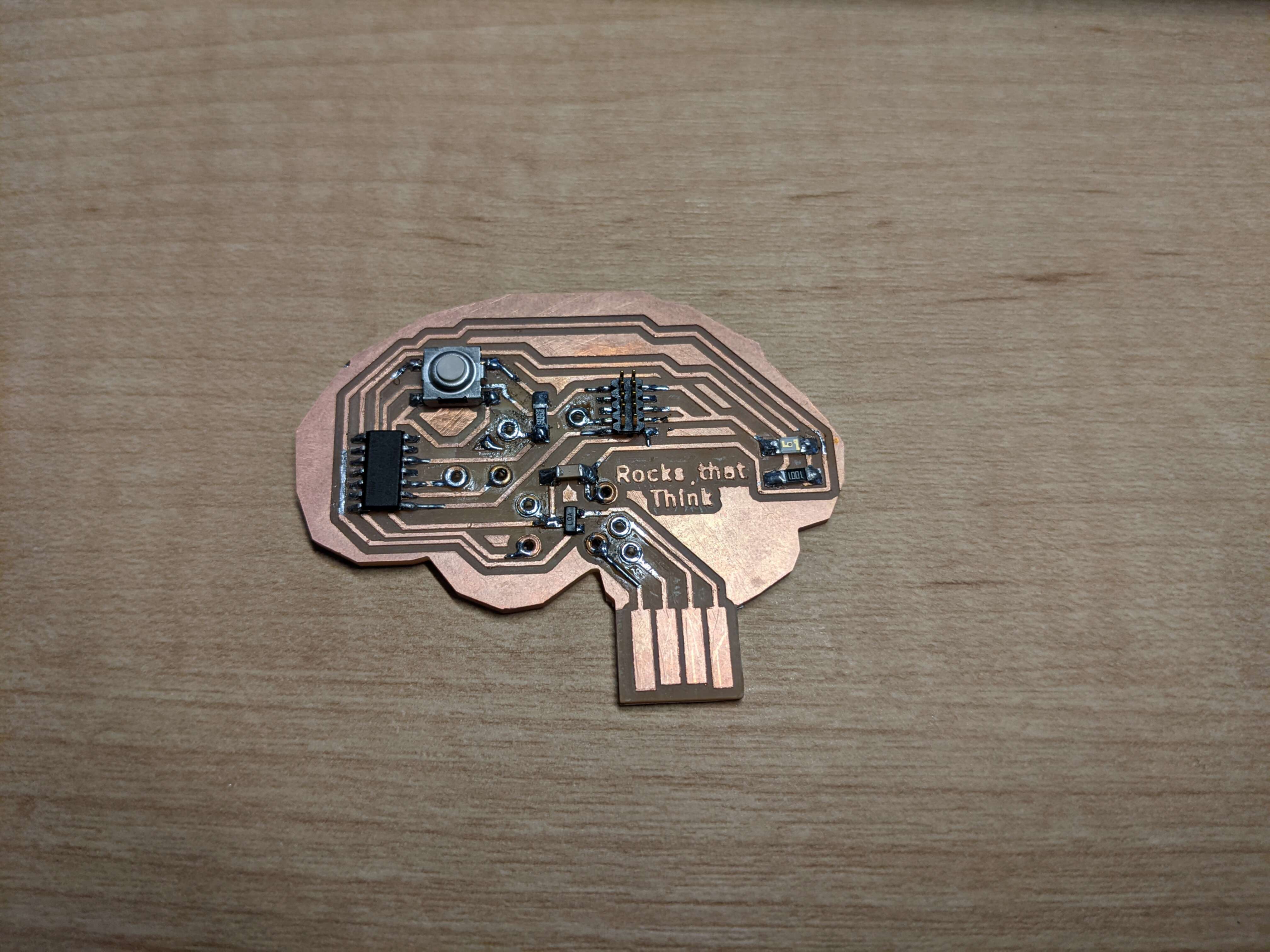
I would show you that it works by running it on my computer, but I unfortunately didn't take any photo proof, so you'll just have to take my word for it.